Quantum Technology Employs Its Capabilities in Electronic Die Sorting
"Rohm Collaborates with Quanmatic to Integrate Quantum Tech in Major Chip Fabrication Plant"
Rohm has partnered with the quantum computing innovator Quanmatic to integrate state-of-the-art quantum technology into a major semiconductor production operation for the first time.

Rohm's production facility in Malaysia
Within the production of semiconductors, the stage of electrical die sorting (EDS) is employed to examine the electrical properties of chipsets on silicon wafers. This phase is pivotal for the assurance of high-quality, dependable devices with high yields. However, due to its intricacy, the EDS process can lead to considerable delays in the manufacturing workflow.
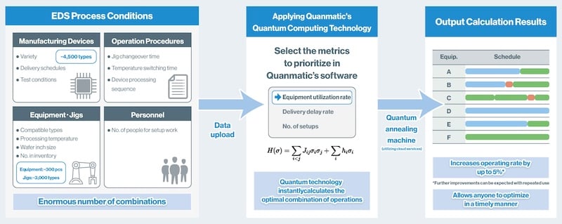
In order to overcome these challenges, Rohm has entered into a fruitful partnership with the quantum technology startup Quanmatic, aiming to streamline the EDS process in the realm of semiconductor manufacturing. Together, they have achieved key efficiency benchmarks in production, setting the stage for the adoption of their innovative approach into large-scale production by the year 2024.
Collaborative Efforts Between Rohm and Quanmatic
Early in 2023, Rohm joined forces with Quanmatic with the intention to harness quantum technology for enhancing the EDS process.
Quantum technology, and specifically the approach known as quantum annealing, has been recognized for its potential in tackling combinatorial optimization issues that span a variety of sectors. In the field of semiconductor production, where the multitude of procedural permutations grows exponentially, quantum technology offers the capability to discover optimal strategies that classical computing could not feasibly solve.
The joint prototype from Rohm and Quanmatic melds the cutting-edge quantum computing solutions from Quanmatic with the comprehensive insight and accumulated data from Rohm.
The EDS process
Testing in Rohm's factories demonstrated significant improvements in key performance indicators like utilization and delivery delay rates, along with reduced computation time.
What Is Electrical Die Sorting?
Electrical die sorting is an essential process in semiconductor manufacturing, strategically positioned between the fabrication step and the packaging phase. It primarily aims to enhance semiconductor yield rates by ensuring each chip meets quality standards before proceeding to subsequent stages. EDS involves several critical steps.
Electrical Test and Wafer Burn-In
The electrical test (ET) involves measuring integrated circuit components' DC voltage and current characteristics to assess nominal operation. Following the ET, the wafer burn-in process heats the wafer and subjects it to AC and DC currents to identify defects, weaknesses, and potential issues, significantly improving product reliability.
Hot/Cold Test
This stage tests the chips at temperatures varying from the norm to identify defective ones. Repairable chips are marked for later correction, ensuring they function flawlessly across different temperature ranges.
Repair/Final Test
Chips deemed repairable in the hot/cold test undergo repairs. A final test confirms the effectiveness of these repairs.
Inking
This final step of the EDS process involves marking defective chips, including those failing the hot/cold test, improperly repaired, or incomplete on the wafer. Defective chips are excluded from assembly, conserving materials, equipment, time, and labor.
Full-Scale Production
EDS is vital for sorting defective semiconductor chips at the wafer level, addressing issues from fabrication or design steps, and streamlining the efficiency of packaging and testing phases. By removing defective chips early, EDS significantly contributes to semiconductor productivity, with yield being a key performance indicator.
This news marks the first instance of quantum technology being employed in a large-scale semiconductor manufacturing facility. With full-scale implementation slated for April 2024, the companies hope to enable a semiconductor supply chain that is continually optimized on a daily basis for better yields and greater throughput.
All images used courtesy of Rohm Semiconductor